


Mã QR

Về chúng tôi
Các sản phẩm
Liên hệ chúng tôi

Điện thoại

Số fax
+86-579-87223657

E-mail

Địa chỉ
Đường Wangda, phố Ziyang, huyện Wuyi, thành phố Kim Hoa, tỉnh Chiết Giang, Trung Quốc


Thin film preparation processes can be divided into two categories according to their film forming methods: physical vapor deposition (PVD) and chemical vapor deposition (CVD), of which CVD process equipment accounts for a higher proportion. Atomic layer deposition (ALD) is one of the chemical vapor deposition (CVD).
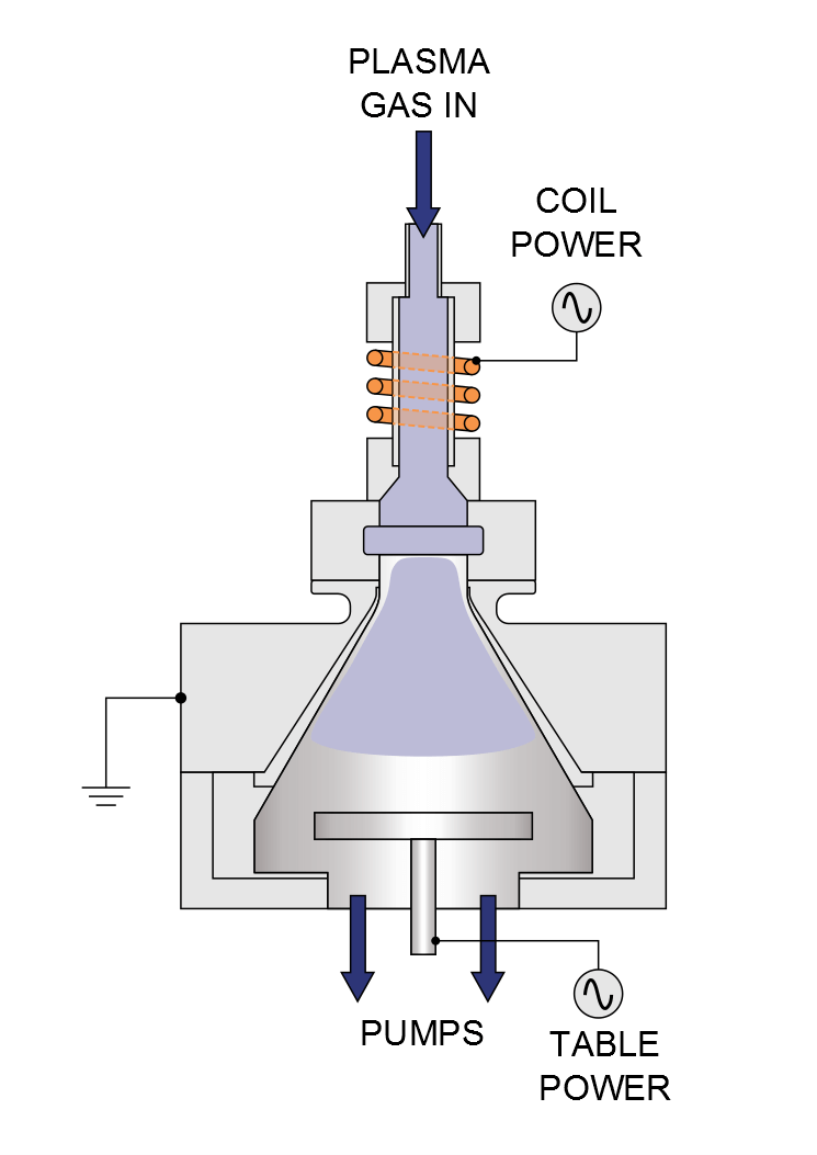
Atomic layer deposition technology (Atomic Layer Deposition, referred to as ALD) is a vacuum coating process that forms a thin film on the surface of a substrate layer by layer in the form of a single atomic layer. ALD technology is currently being widely adopted by the semiconductor industry.
Atomic layer deposition process:
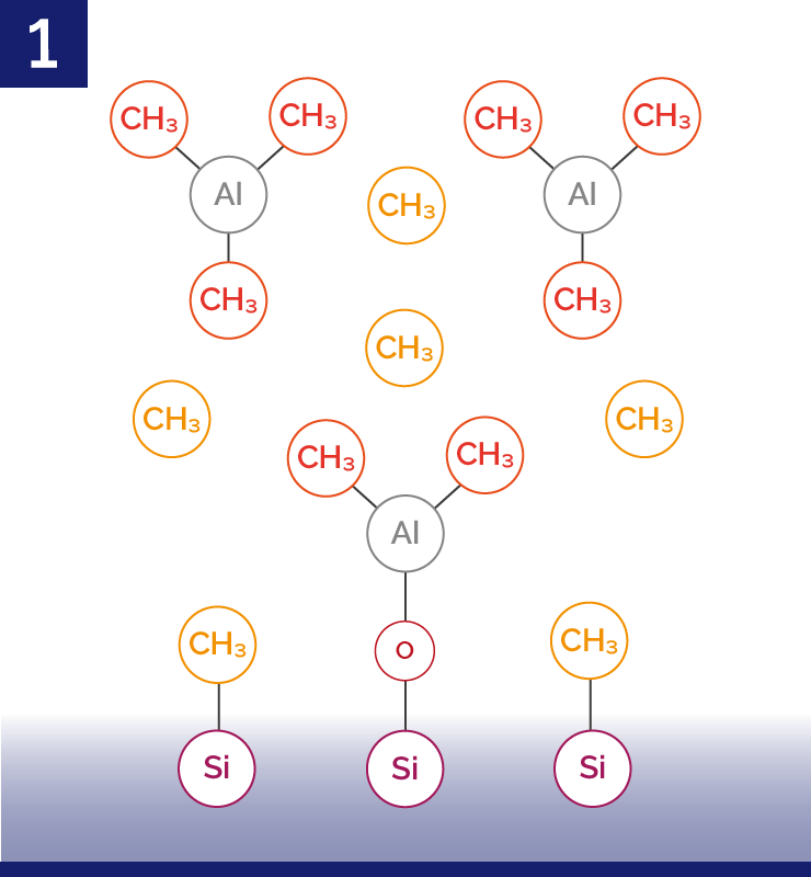
Atomic layer deposition usually includes a cycle of 4 steps, which is repeated as many times as needed to achieve the required deposition thickness. The following is an example of ALD of Al₂O₃, using precursor substances such as Al(CH₃) (TMA) and O₂.
Step 1) Add TMA precursor vapor to the substrate, TMA will adsorb on the substrate surface and react with it. By selecting appropriate precursor substances and parameters, the reaction will be self-limiting.
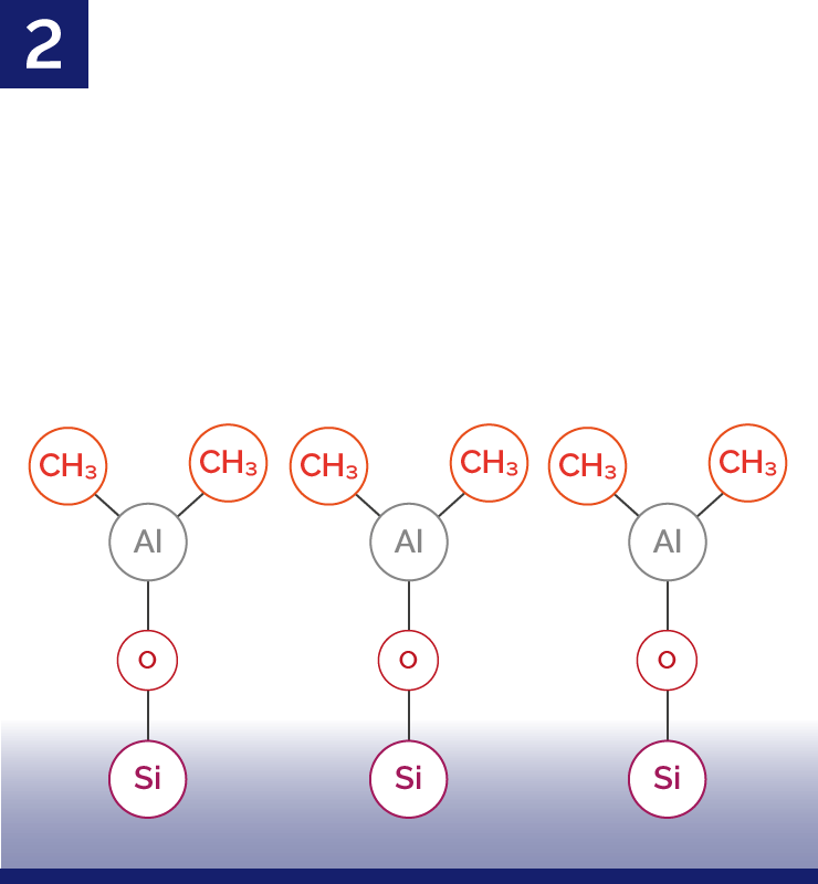
Step 2) Remove all residual precursors and reaction products.
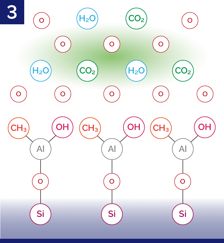
Step 3) Low-damage remote plasma irradiation of the surface with reactive oxygen radicals oxidizes the surface and removes surface ligands, a reaction that is also self-limiting due to the limited number of surface ligands.
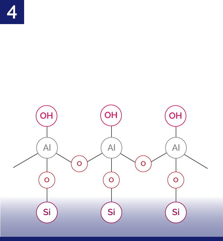
Step 4) Reaction products are removed from the chamber.
Only step 3 differs between thermal and plasma processes, with H₂O being used in thermal processes and O₂ plasma being used in plasma processes. Since the ALD process deposits (sub)-inch-thick films per cycle, the deposition process can be controlled at the atomic scale.
Highlights of Atomic Layer Deposition (ALD):
1) Grow high-quality thin films with extreme thickness accuracy, and only grow a single atomic layer at a time
2) Wafer thickness can reach 200 mm, with typical uniformity <±2%
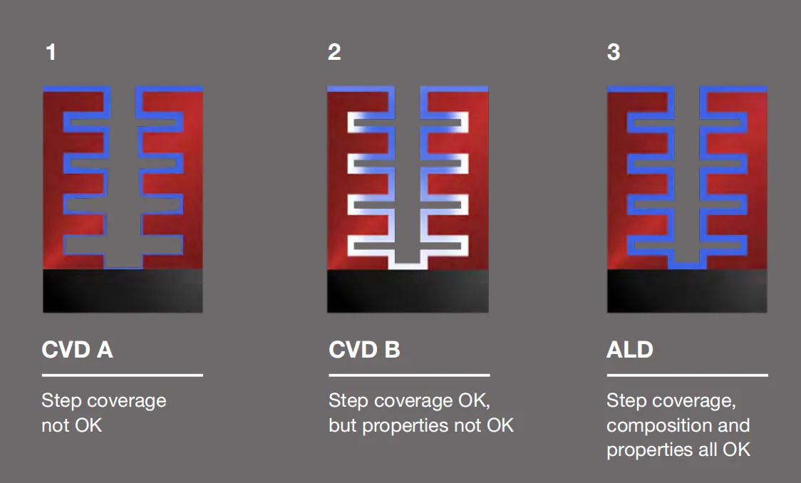
3) Excellent step coverage even in high aspect ratio structures
4) Highly fitted coverage
5) Low pinhole and particle levels
6) Low damage and low temperature process
7) Reduce nucleation delay
8) Applicable to a variety of materials and processes
Compared with traditional chemical vapor deposition (CVD) and physical vapor deposition (PVD), the advantages of ALD are excellent three-dimensional conformality, large-area film uniformity, and precise thickness control, etc. It is suitable for growing ultra-thin films on complex surface shapes and high aspect ratio structures. Therefore, it is widely applicable to substrates of different shapes and does not require control of reactant flow uniformity.
Comparison of the advantages and disadvantages of PVD technology, CVD technology and ALD technology:
|
PVD technology |
CVD technology |
ALD technology |
|
Faster deposition rate |
Average deposition rate |
Slower deposition rate |
|
Thicker film thickness, poor control of nano-level film thickness precision |
Medium film thickness (depends on the number of reaction cycles) |
Atomic-level film thickness |
|
The coating has a single directionality |
The coating has a single directionality |
Good uniformity of large-area film thickness |
|
Poor thickness uniformity |
Average step coverage |
Best step coverage |
|
Poor step coverage |
\ |
Dense film without pinholes |
Advantages of ALD technology compared to CVD technology (Source: ASM)
Vetek Semiconductor is a professional ALD Susceptor products supplier in China. Our ALD Susceptor, SiC coating ALD susceptor and ALD Planetary Susceptor are widely used in key components of semiconductor manufacturing equipment. Vetek Semiconductor is committed to providing advanced and customizable ALD Susceptor products and technical solutions of various specifications for the semiconductor industry. We sincerely look forward to becoming your supplier in China.


+86-579-87223657
Đường Wangda, phố Ziyang, huyện Wuyi, thành phố Kim Hoa, tỉnh Chiết Giang, Trung Quốc